Synthetic diamonds are quietly rescuing modern electronics from thermal collapse. Semiconductor manufacturing faces a hard physical wall as microchips shrink, pushing heat dissipation to the absolute limit. Traditional heat spreaders made from copper and aluminum fail to keep pace with extreme power densities. Pure carbon crystal lattices change that equation entirely. By combining artificial gem production with machine learning optimization, material scientists have unlocked a method to cool next-generation processors efficiently. The convergence of synthetic diamond production and thermal engineering addresses the most urgent physical bottleneck in modern computing.
Silicon has reached its twilight. Engineers cram billions of transistors onto fingernail-sized dies, generating heat fluxes that rival the surface of the sun. When processors overheat, performance throttles, leakage current spikes, and silicon degrades permanently. Traditional cooling solutions rely on fluid loops, vapor chambers, and metallic heatsinks. Those methods hit a thermodynamic ceiling years ago.
Carbon offers an escape hatch. Diamond possesses a thermal conductivity roughly five times higher than copper. Heat moves through a diamond lattice at incredible speeds, dragging thermal energy away from delicate gate structures before localized hotspots can melt the silicon. Until recently, using diamonds in consumer or enterprise hardware remained economically unviable. Growing single-crystal gem material required weeks inside high-pressure, high-temperature chambers, yielding tiny stones riddled with structural flaws.
The economic calculus shifted dramatically over the past thirty years. Industrial diamond synthesis moved from a niche scientific curiosity to a high-volume manufacturing sector. Chemical vapor deposition changed the trajectory of the entire industry. Technicians feed carbon-rich gases into a vacuum reactor, igniting a plasma ball that forces carbon atoms to rain down onto a substrate, stacking atomic layers into a pure crystal.
Scaling this process for semiconductor integration demanded precision that human operators struggled to maintain. Small pressure fluctuations or minute temperature variations inside the reactor ruin an entire batch, turning premium electronic-grade material into worthless carbon soot.
Machine learning entered the workflow out of sheer desperation. Human engineers could no longer manually tune the hundreds of variables dictating plasma stability and crystal growth rates. Neural networks now monitor reactor chambers in real time. Algorithms ingest millions of data points per second, adjusting gas flow, microwave power, and substrate temperature autonomously.
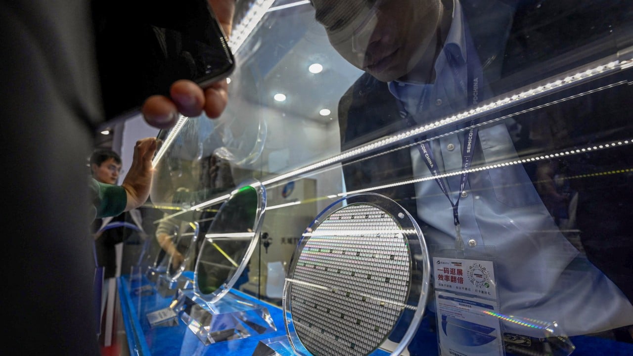
This technological marriage yields synthetic diamond wafers with unprecedented purity and thermal performance. Artificial intelligence identifies microscopic crystal defects milliseconds after formation, correcting anomalies before structural integrity fails. The result is a steady supply of large-area diamond plates suitable for direct integration onto high-power gallium nitride and silicon carbide semiconductors.
The demand surge originates far outside the jewelry market. Artificial intelligence data centers consume staggering amounts of electricity, converting most of that power directly into waste heat. Graphics processing units running large language models burn through thermal envelopes in seconds. Hyperscale operators spend fortunes on liquid cooling infrastructure, pumping chilled water through racks of servers.
Liquid cooling treats symptoms rather than the root cause. It moves heat away from the chip, but the bottleneck remains at the interface between the silicon die and the cooling block. Inserting a synthetic diamond layer directly above the hot spots alters the thermodynamics entirely. Thermal resistance plummets. Chips run cooler at higher clock speeds, consuming less energy overall.
Automotive manufacturers face identical thermal constraints. Electric vehicle inverters handle hundreds of kilowatts of power, converting battery DC current into AC drive signals for the motors. Power modules built with silicon carbide fail prematurely if junction temperatures spike. Embedding diamond substrates into these power modules extends operational lifespans exponentially, reducing failure rates in demanding environments.
The Manufacturing Reality Behind the Hype
Commercializing advanced materials sounds glamorous in corporate press releases. The factory floor tells a different story. Growing high-purity electronic-grade diamond via chemical vapor deposition is an agonizingly slow and energy-intensive procedure.
Reactors run continuously for weeks to produce a single thick wafer. Power grids bear the brunt of this industrial appetite. Generating the plasma required for diamond synthesis demands massive electrical inputs. If the electricity powering the reactor comes from fossil fuels, the green credentials of the final electronic device shrink considerably. Analysts tracking the sector often gloss over this carbon paradox. Producing a material designed to save energy consumes vast amounts of energy upfront.
Yield rates present another persistent hurdle. Even with advanced machine learning oversight, thermal stress during the cooling phase can cause diamond wafers to fracture spontaneously. Carbon atoms want to form specific bonds, but imperfections in the seed crystal multiply as the layer thickens. A wafer measuring four inches in diameter represents a monumental achievement in materials science, yet commercial viability requires eight-inch or twelve-inch formats to match existing semiconductor fabrication lines.
Bridging that gap requires rethinking crystal growth fundamentals. Researchers are experimenting with heteroepitaxy, growing diamond layers on foreign substrates like silicon or iridium rather than expensive diamond seed plates. Mismatched crystal lattices create intense mechanical strain, often causing the diamond film to delaminate. Machine learning algorithms currently map these strain fields, predicting where cracks will propagate and altering growth parameters dynamically to relieve internal tension.
The economic pressure to succeed is intense. Venture capital flows into startups promising revolutionary thermal substrates, driving valuations skyward. A few firms will deliver functional products at scale. Many others will burn through capital trying to scale up brittle carbon chemistry.
Integration Nightmares in the Fab
Designing a diamond heat spreader is one challenge. Integrating it into an established semiconductor packaging line is an engineering nightmare.
Semiconductors rely on lithography, etching, and metal deposition techniques perfected over half a century of silicon manufacturing. Diamond does not play nicely with traditional cleanroom processes. It resists chemical etching. Cutting a diamond wafer into precise geometries requires expensive laser ablation, introducing microscopic thermal damage along the cutting edges.
Thermal boundary resistance remains a persistent thorn in the side of packaging engineers. Even if a diamond plate possesses infinite thermal conductivity, the microscopic gap between the silicon die and the diamond layer acts as a thermal barrier. Bonding these two dissimilar materials requires specialized interfacial layers, often utilizing titanium or gold metallization schemes. Every additional interface introduces thermal resistance, eroding the theoretical advantages of carbon-based cooling.
Engineers must also account for the thermal expansion coefficient mismatch. Silicon and diamond expand at different rates when heated. As a high-performance processor cycles between idle and full load, the mechanical stress at the bonding interface builds relentlessly. Without careful buffer layer design, the diamond plate simply shears off the silicon die after a few thousand power cycles.
Addressing these integration hurdles demands cross-disciplinary collaboration between metallurgists, software developers, and packaging specialists. Companies treating synthetic diamond as a drop-in replacement for copper will fail. Success requires redesigning the entire package architecture from the silicon up.
The Global Supply Chain Shift
Geopolitics rarely stays out of critical material supply chains. The geographic concentration of synthetic diamond manufacturing is shifting rapidly. For decades, traditional gem-quality synthesis was dominated by producers in specific Asian hubs and select Western laboratories.
Electronic-grade diamond production requires specialized equipment, proprietary recipes, and strict quality control protocols. Nations view thermal management materials as strategic assets. High-power military radar, aerospace electronics, and quantum computing infrastructure all rely on advanced semiconductors that generate extreme heat. Controlling the supply of high-purity diamond wafers translates directly to technological sovereignty.
Export controls on high-end chemical vapor deposition reactors and microwave generators are tightening. Governments recognize that whoever controls advanced thermal management controls the future of high-performance computing. Startups operating in this space find themselves navigating complex trade regulations and intellectual property protection hurdles.
The market splits into distinct tiers. Luxury jewelry producers fight for consumer disposable income using lab-grown stones as an ethical alternative to mined diamonds. Industrial producers ignore the jewelry market entirely, focusing on nitrogen-vacancy centers for quantum sensing and high-purity plates for power electronics. The equipment used for electronic-grade material bears little resemblance to consumer gem reactors. The purity requirements are orders of magnitude higher, demanding ultra-clean vacuum chambers and meticulous feedstock gas filtration.
Investors often confuse the two markets, driving wild market swings based on retail jewelry trends rather than industrial semiconductor demand. Analysts who understand the technical distinction look past consumer pricing pressure and focus entirely on reactor throughput and wafer defect density metrics.
Looking Past the Horizon
The trajectory of electronic cooling points toward total material reinvention. As gate-all-around transistors and three-dimensional stacked dies become standard, cooling from the outside in will no longer suffice. Thermal management must happen at the atomic level, embedded directly within the active layers of the processor.
Researchers are already exploring microscopic diamond cooling channels etched directly into the back-side of silicon wafers, circulating dielectric fluids through diamond micro-architectures. This approach merges fluid dynamics with solid-state physics, pushing performance boundaries previously thought impossible.
The physical limits of silicon are non-negotiable. Thermodynamics does not negotiate, and heat refuses to be ignored. Synthetic diamond, guided by predictive machine learning algorithms and refined through decades of industrial persistence, provides the only viable path forward for high-density computing. The transition will be messy, expensive, and unforgiving to companies lacking deep technical expertise. The silicon squeeze is here, and carbon is the only material tough enough to break it.